Winwon Chips Winwon Chips

Original New Integrated Circuit Passive Active Electronic Component Supplier

Still deciding? Get samples of $ !
Order Sample

Product Description

Basic Information

Model NO.
Component
Layers
Multilayer
Base Material
FR-4
Certification
RoHS, CCC, ISO
Customized
Customized
Board Size
Customization
Copper Thickness
0.5-6 Oz
Service
PCB & PCBA One-Stop Turnkey Service
Layer Range
1-60 Layers
Surface Finishing
OSP, Lead Free HASL, ENIG, Immersion Tin, Gold PLA

Packaging & Delivery

Package Size
20.00cm * 20.00cm * 20.00cm
Gross Weight
5.000kg

Product Advantages

Powerful Production Capacity

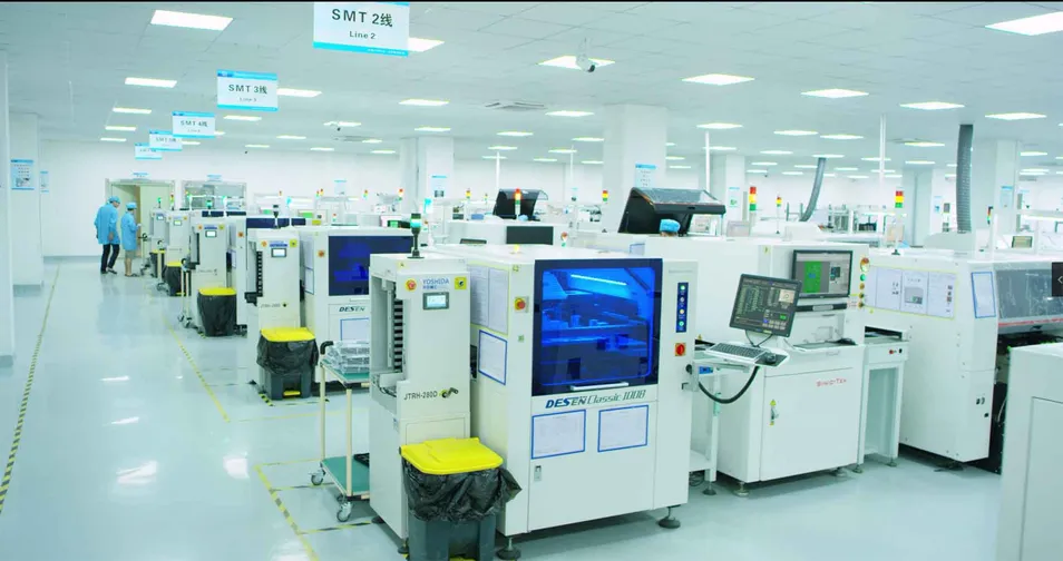
Equipped with 7 fully automatic SMT lines and 3 DIP lines, our facility supports a full spectrum of manufacturing requirements—from rapid prototyping to high-volume mass production. These advanced lines enable high-speed, high-precision component placement, stable throughput, and consistent product quality.

Production Facility
SMT Line
Electronic Components
Full Supply Chain Management

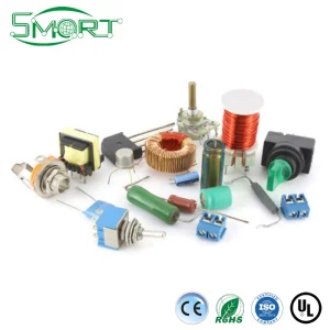
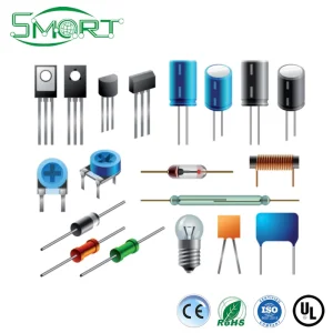
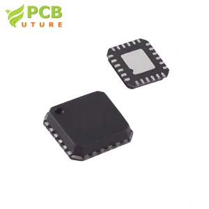
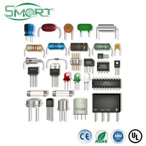
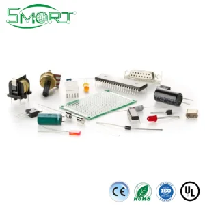
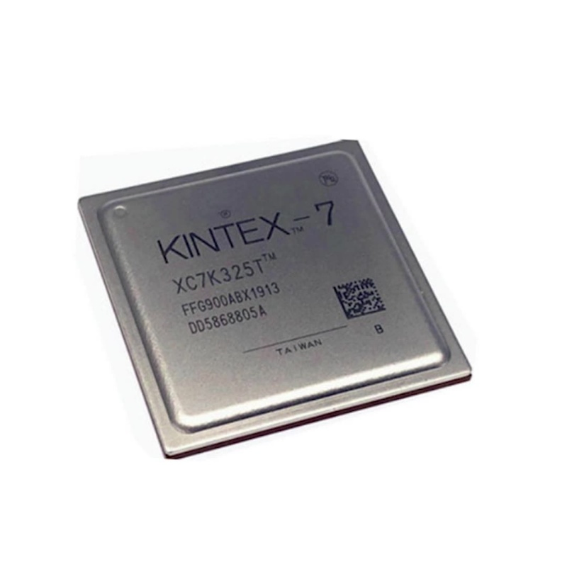
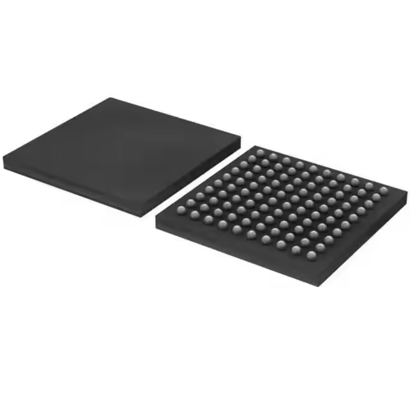
We specialize in comprehensive Components Sourcing and CKD (Completely Knocked Down) Kits management. We collaborate with authorized dealers and franchise partners of major semiconductor brands including Texas Instruments, STMicroelectronics, Microchip, Infineon, and Analog Devices. These diversified sourcing channels ensure supply stability, full traceability, and guaranteed authenticity of all components.

Quality Assurance

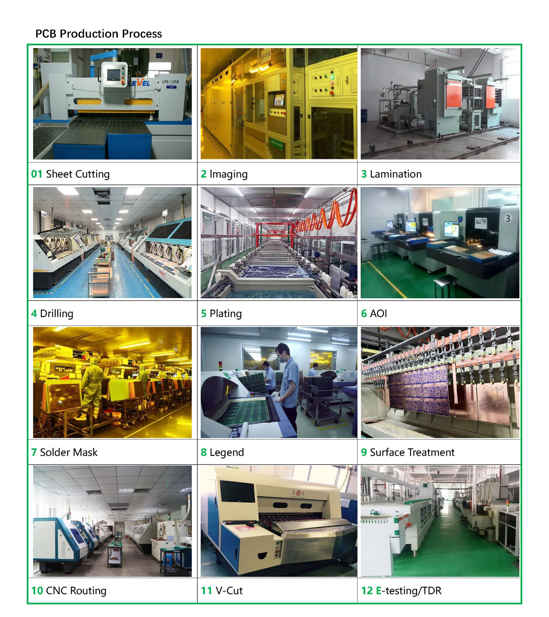
ISO9001, UL, RoHS, and TS16949 certified. Every board undergoes a complete suite of inspections, including AOI for visual accuracy, X-Ray for high-density component validation, and ICT testing for electrical performance. This framework ensures each product meets rigorous reliability and durability requirements.

Technical Capabilities

PCB Capability
FeaturesRigid PCBFLEX PCBRIGID-FLEX PCB
Max Layer42L8L36L
Max. Panel Size600*770mm500*1200mm500*1200mm
Inner Min Trace/Space2.5/2.5mil3/3mil3/3mil
Board Thickness0.4-11.5mm0.1-0.5mm0.4-8mm
Surface TreatmentENIG, Gold Finger, Immersion Silver/Tin, HASL LF, OSP, ENEPIG
PCB Assembly Capability
1Single and double sided SMT/PTHYes
2Min Chips size01005
3Min BGA pitch0.2mm
4Max PCB size14.5 in.x 19.5 in.
5InspectionX-ray / AOI testing / ICT

Manufacturing Flow

PCB Process Flow

PCB Production

  • Engineering Review (DFM/CAM)
  • Inner Layer Imaging & Etching
  • Lamination & Drilling
  • Copper Plating & Via Metallization
  • Solder Mask & Surface Finishing
  • Electrical Testing & Final Inspection

PCBA Production

  • Solder Paste Printing & SPI
  • SMT Pick-and-Place
  • Reflow Soldering & AOI
  • DIP / Through-Hole Insertion
  • X-Ray & Functional Test (FCT)
  • ESD Packaging & Shipping

Application Fields

Applications
Consumer Electronics: Smartphones, wearables, and smart home devices.
Industrial Automation: PLCs, motor controllers, and IIoT equipment.
Automotive: ECU modules, ADAS systems, and BMS.
Medical: Diagnostic instruments and portable medical equipment.
Communications: 5G infrastructure, routers, and RF equipment.
Aerospace & Defense: Navigation systems and robust control modules.

Frequently Asked Questions

What is needed for a quotation?
Please provide the Gerber file for PCB manufacturing, and the BOM list (Bill of Materials) for components sourcing and assembly.
Do you accept small orders?
Yes, we welcome both prototype orders (MOQ 1-5 pcs) and mass production.
How do you ensure component quality?
We only source from authorized distributors and original manufacturers. No fake parts allowed.
What is your typical lead time?
PCB fabrication usually takes 3–7 days, and PCBA assembly 7–15 days depending on complexity and component availability.
Can you handle BGA, QFN, or fine-pitch assembly?
Yes, our SMT lines support BGA, QFN, 01005, and other advanced packaging with X-Ray verification.
How do you protect customer data?
All files are kept strictly confidential, and we sign NDAs upon request to safeguard your designs.

Related Products